
A Practical Directory of Semiconductor Packaging and Test Partners
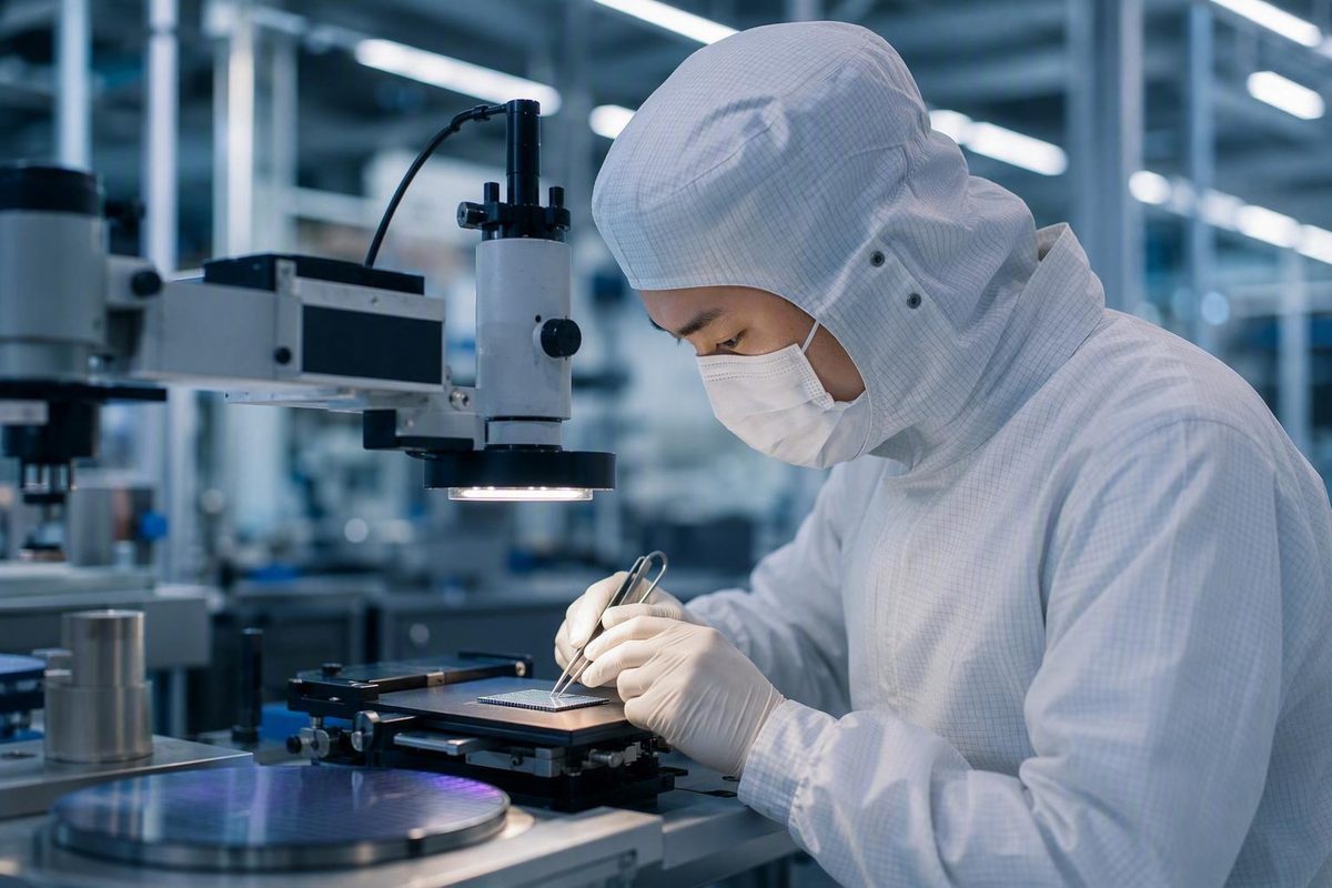
KYEC is better classified as test-focused than full-service. Compare niche providers by package technology, application and facility checks.
A useful specialized semiconductor packaging and testing companies list should help a buyer build a defensible shortlist—not suggest that every listed business is interchangeable. Full-service outsourced semiconductor assembly and test providers, dedicated test houses, high-reliability specialists, turnkey ASIC firms, foundries, equipment manufacturers, and materials suppliers occupy different positions in the semiconductor supply chain.
This directory separates those categories and maps documented capabilities to package technologies and applications. It is the beginning of supplier qualification, not a substitute for facility-level technical review, quality audits, commercial negotiation, legal and trade-compliance advice, or a formal request for quotation.
How to read this semiconductor packaging and testing companies list
This is a non-exhaustive supplier-discovery list, not an authoritative worldwide directory and not an ordinal ranking.
Research reviewed: August 17, 2026. This date reflects review of the supplied evidence, not direct verification of each provider’s current facilities, certifications, customer access, production readiness, or available capacity.
The primary inclusion group consists of companies explicitly described in the available evidence as providing semiconductor assembly, packaging, testing, or a documented combination of those services.
Five provider-type labels are used:
- Full-service OSAT: A third-party provider documented as offering semiconductor assembly or packaging together with testing.
- Test-focused provider: A company whose clearest documented role is wafer probe, production test, burn-in, characterization, or another test function.
- Niche packaging or high-reliability specialist: A provider oriented toward specialized technologies, qualification work, lower-volume programs, or demanding applications.
- Turnkey ASIC partner: A company that includes packaging or testing within a broader design-to-manufacturing program.
- Adjacent semiconductor participant: A foundry, integrated manufacturer, equipment company, materials supplier, substrate business, research organization, or information service that should not automatically receive an OSAT RFQ.
Each directory entry also receives one of these service-status markers:
- Packaging and testing documented
- Testing documented
- Packaging documented
- Scope requires direct verification
- Not documented as an outsourced packaging-and-test provider
“Documented” means that the service appears in the supplied secondary evidence. It does not mean the capability has been independently audited. Most descriptions come from market-research pages, distributor articles, industry publications, or commercial vendor directories. Some directory profiles may have been supplied or influenced by the vendor.
The evidence grades used in the tables are:
- Repeated secondary support: The classification or capability appears across multiple supplied sources.
- Single secondary source: One supplied article or market page supports the claim.
- Directory-supplied description: A commercial directory lists the service, but independent verification is not supplied.
- Direct verification required: The available evidence is incomplete, broad, or insufficient to establish the full production scope.
The article does not rank companies by revenue. Published OSAT tables use approximate estimates that may cover total corporate operations rather than packaging-and-testing revenue alone. Consolidated amounts may include acquired businesses, while other figures may represent standalone companies. Some rankings also combine broad OSAT businesses with KYEC even though the same evidence characterizes KYEC primarily as a testing provider.
Before issuing an RFQ, record the date of the supplier research and verify:
- Current ownership and operating identity
- Active facilities and the work performed at each
- Supported package processes and test platforms
- Current quality and sector-specific certifications
- Prototype, ramp, and production-volume support
- Operational and commercially available capacity
- Customer-access and trade-compliance restrictions
- Whether each operation is internal or subcontracted
- Ownership of tooling, test programs, data, and work product
Legacy names need particular care. An acquired brand may remain visible in older directories without representing an independent sourcing alternative.
What OSAT, packaging, assembly, and semiconductor testing mean
OSAT stands for outsourced semiconductor assembly and test. An OSAT performs backend services for semiconductor devices fabricated by a foundry or integrated device manufacturer.
A simplified backend flow can include:
- Wafer probing or wafer sort
- Wafer preparation, thinning, or related processing where required
- Dicing or singulation
- Die attachment
- Electrical interconnection through wire bonding, flip-chip bonding, or another method
- Encapsulation or package assembly
- Marking and package singulation
- Burn-in where required by the product or qualification plan
- Final electrical test
- Reliability qualification, yield analysis, or failure analysis
The exact sequence depends on the device and package architecture. Some operations occur while devices remain in wafer form; others occur after individual die or packages have been assembled.
Conventional and advanced packaging
Conventional packaging generally refers to mature structures and assembly methods such as lead-frame packages, wire-bonded devices, and established laminate-based formats. “Conventional” does not mean technically trivial or inappropriate for demanding products. Mature processes may be preferable when cost, supply availability, qualification history, or production stability matters more than maximum interconnect density.
Advanced packaging moves more system integration into the backend. It can include:
- Flip-chip
- Wafer-level packaging
- Fan-out packaging
- System-in-package
- Through-silicon vias
- Silicon or organic interposers
- 2.5D integration
- 3D stacking
- Chiplets
- Hybrid bonding
- Heterogeneous integration
These approaches can combine multiple dies, functions, process technologies, or component types in one package or integrated assembly. McKinsey describes wafer-level fan-in and fan-out, 2.5D stacking, 3D stacking, and hybrid bonding while connecting packaging’s growing importance to the limits of front-end scaling in its advanced-chip-packaging analysis.
Packaging is not the same as testing
A company’s ability to assemble an advanced package does not establish that it offers wafer probe, burn-in, qualification, or production final test.
Semiconductor test services can include:
-
Wafer probe or sort: Electrically evaluating die while they remain on the wafer.
-
Test-program development: Creating and validating the software and hardware interfaces required for automated test.
- Reliability qualification: Executing defined stress and evaluation plans.
- Failure analysis: Investigating why a device, package, or process failed.
- Yield analysis: Studying manufacturing and test data to identify loss patterns and improvement opportunities.
A foundry manufactures wafers and may provide integrated packaging platforms. An integrated device manufacturer may have internal fabrication and packaging capabilities. Neither category is automatically an independent OSAT. Equipment and materials companies enable packaging and test operations but generally do not perform outsourced production merely because they participate in the same market.
Core full-service OSAT and assembly-and-test providers
The following table normalizes company descriptions from the supplied evidence. ASE Technology, Amkor Technology, and JCET Group have the strongest cross-source support as independent packaging-and-test providers. The other entries should not be assumed to have equivalent scale, technology breadth, geographic reach, or evidence depth.
| Company | Provider type | Service status | Documented packaging capabilities | Documented testing capabilities | Applications or specialties attributed by sources | Stated headquarters | Evidence basis |
|---|---|---|---|---|---|---|---|
| ASE Technology | Full-service OSAT | Packaging and testing documented | Fan-out, SiP, 2.5D and multi-die solutions | IC and production testing | AI, HPC, communications and heterogeneous integration | Taiwan | Repeated secondary support in an OSAT comparison |
| Amkor Technology | Full-service OSAT | Packaging and testing documented | Flip-chip, wafer-level packaging, SiP and automotive packaging | Semiconductor testing | Automotive, mobile and high-density packages | United States | Repeated secondary support in an IC packaging-and-testing market profile |
| JCET Group | Full-service OSAT | Packaging and testing documented | Advanced IC packaging and chiplet-related approaches | IC testing | Integrated packaging-and-test programs | China | Repeated secondary support in an advanced-packaging company comparison |
| Tongfu Microelectronics | Full-service OSAT | Packaging and testing documented | Advanced packaging, flip-chip and chiplet-related backend work | Testing | Complex backend programs | China | Secondary support in an OSAT company overview |
| Powertech Technology | Full-service OSAT | Packaging and testing documented | Memory packaging; reported logic, TSV and fan-out panel-level expansion | Semiconductor testing | DRAM, NAND and memory products | Taiwan | Secondary support in the same cited OSAT overview |
| Huatian Technology | Full-service OSAT | Packaging and testing documented | Lead-frame, fan-out and TSV packaging | Testing at company-category level | Broad IC packaging | China | Secondary-source support; detailed limits not supplied |
| UTAC | Full-service OSAT | Packaging and testing documented | IC assembly and packaging | Testing | Automotive, industrial, analog, mixed-signal, sensors and power management | Not relied on here | Secondary support in the cited advanced-packaging comparison |
| ChipMOS | Full-service OSAT | Packaging and testing documented | Memory and display-driver packaging, chip-on-film and chip-on-glass | Assembly and testing | Memory and display-driver ICs | Taiwan | Focused support in the cited OSAT comparison |
| Chipbond | Full-service OSAT | Packaging and testing documented | Display-driver packaging; gold or solder bumping | Testing | Display-driver ICs and bumping | Taiwan | Focused secondary support; broader scope requires verification |
ASE Technology
ASE is one of the clearest independent OSAT candidates in the supplied evidence. Sources associate it with packaging and testing, including fan-out, system-in-package, 2.5D, and multi-die solutions.
That breadth makes ASE a reasonable discovery-stage candidate for complex integration programs. It does not prove that a particular facility supports a buyer’s required interposer, substrate, die count, package size, thermal envelope, test flow, schedule, or production volume.
Amkor Technology
Amkor is consistently described as an outsourced assembly-and-test provider. Documented associations include flip-chip, wafer-level packaging, SiP, automotive packaging, and semiconductor testing.
Its association with automotive packaging should not be interpreted as automatic qualification for a particular component, customer standard, or production site. Those details require current facility records, certificates, process documentation, and product-specific qualification evidence.
JCET Group
JCET is documented as an integrated-circuit packaging-and-test provider with advanced-packaging and chiplet-related capabilities. Buyers should verify which legal entity and facility would contract for and execute the proposed work.
Older references to acquired operations should not be treated as proof that legacy brands remain separate sourcing alternatives.
Tongfu Microelectronics
Tongfu Microelectronics is associated with advanced packaging, flip-chip, chiplet-related backend work, and testing. It is a potential candidate for complex backend programs, subject to confirmation of process availability, test coverage, commercial access, applicable trade restrictions, and facility-level qualifications.
Powertech Technology
Powertech Technology is associated with packaging and testing for memory products, particularly DRAM and NAND. The evidence also reports expansion into logic packaging, TSV, and fan-out panel-level packaging.
A buyer should distinguish among historical specialization, announced development, qualified production, and capacity currently available to new customer programs.
Huatian Technology
Huatian Technology is described as a packaging-and-testing provider associated with lead-frame, fan-out, and TSV packaging. The evidence does not provide the package dimensions, pitches, wafer sizes, thermal limits, test platforms, facility qualifications, or available capacity needed for supplier selection.
UTAC
UTAC is associated with assembly and testing for automotive, industrial, analog and mixed-signal, sensor, and power-management products. The supplied evidence also associates UTAC with Wise Road ownership following an acquisition.
Ownership, contracting entity, operating sites, certifications, and current service availability should be confirmed before comparing UTAC with other OSATs.
ChipMOS and Chipbond
ChipMOS is a focused candidate for memory and display-driver IC assembly, packaging, and testing, including chip-on-film and chip-on-glass work. Chipbond is associated with display-driver packaging and testing as well as gold or solder bumping.
Chipbond’s broader production scope is less clearly established. Buyers should confirm whether a required flow extends beyond bumping and driver-IC-related operations.
Additional assembly-and-test candidates
A market-research directory also names the following companies as packaging, assembly, or testing providers. Its tier methodology is not disclosed, so these entries are leads for investigation rather than evidence of equivalent scale or capability.
| Company | Provider type | Service status | Documented association | Evidence grade |
|---|---|---|---|---|
| Hana Micron | Full-service OSAT | Packaging and testing documented | Flip-chip, advanced packages and testing | Single secondary source |
| Unisem | Full-service OSAT candidate | Scope requires direct verification | Packaging, assembly, or testing provider | General secondary-source association |
| Carsem | Full-service OSAT candidate | Scope requires direct verification | Packaging, assembly, or testing provider | General secondary-source association |
| Walton Advanced Engineering | Full-service OSAT candidate | Scope requires direct verification | Packaging, assembly, or testing provider | General secondary-source association |
| Sigurd Microelectronics | Full-service OSAT candidate | Scope requires direct verification | Packaging, assembly, or testing provider | General secondary-source association |
| Lingsen Precision Industries | Full-service OSAT candidate | Scope requires direct verification | Packaging, assembly, or testing provider | General secondary-source association |
The cited market page identifies these businesses within its packaging, assembly, and testing company lists, but the supplied text does not explicitly establish both outsourced packaging and testing for every entry. They should therefore not be treated as equal in technology, scale, customer access, or evidence quality.
Test-focused and specialist packaging providers
Large OSATs are not automatically the best fit for characterization, engineering lots, unusual test conditions, qualification programs, or low-volume high-reliability products. A narrower specialist may provide a more suitable service model.
The commercial directory used for several entries includes companies with widely different business models, from RF validation firms to turnkey ASIC partners and high-reliability microelectronics providers. Directory inclusion does not establish capacity, certifications, quality, or suitability.
| Company | Provider type | Service status | Documented focus | Principal verification issue |
|---|---|---|---|---|
| KYEC | Test-focused provider | Testing documented | Wafer probing, final test, burn-in and complex-device testing | Do not assume end-to-end packaging |
| Integra Technologies | Niche packaging or high-reliability specialist | Packaging and testing documented | Complex assembly and test for critical applications | Confirm facility, certifications and customer access |
| Micross | Niche packaging or high-reliability specialist | Packaging and testing documented | OSAT services, advanced packaging, wafer processing, test, qualification and component modification | Validate exact internal flow and site |
| Presto Engineering | Niche packaging or high-reliability specialist | Packaging and testing documented | RF and mixed-signal testing, packaging, qualification, failure analysis and backend production | Confirm production volume and platform limits |
| RoodMicrotec | Test-focused provider | Testing documented | Device test, program development, qualification, reliability, failure analysis and end-of-line services | Packaging breadth requires verification |
| NHanced Semiconductors | Niche packaging or high-reliability specialist | Packaging documented | Wafer reconstruction, optical and RF interposers, MEMS and 3D designs | Complete outsourced test portfolio not established |
| TMS Test Services | Test-focused provider | Testing documented | RF semiconductor validation and on-wafer work | Not documented as a packaging provider |
| Neways Advanced Microsystems | Niche packaging or high-reliability specialist | Packaging documented | Packaging and assembly for MEMS and sensors in harsh environments | Full production-test scope not established |
| SYNERGIE CAD PSC | Niche packaging or high-reliability specialist | Packaging and testing documented | IC packaging, testing, qualification and industrialization | Directory-supplied description requires validation |
| Caliber Interconnect Solutions | Turnkey ASIC partner | Testing documented | Wafer and final testing plus package and substrate design | Package design does not prove production assembly |
| Alphacore | Turnkey ASIC partner | Testing documented | Analog, mixed-signal, RF, imaging and radiation-hardened testing | Production packaging scope not established |
The Micross, Presto Engineering, RoodMicrotec, TMS, Neways, SYNERGIE CAD PSC, Caliber, and Alphacore descriptions come from a commercial semiconductor-testing vendor directory. Those profiles should be validated against current company documents and the proposed operating site.
KYEC
King Yuan Electronics, generally abbreviated KYEC, is better classified as a test-focused provider than automatically grouped with full-service OSATs. The supplied evidence associates it with wafer probing, final testing, burn-in, and complex GPU-related test work.
KYEC may be relevant when the sourcing problem is test capacity or engineering expertise rather than package assembly. An RFQ should identify device power, frequency, temperature, handler requirements, test time, parallelism, interface hardware, data format, and ownership of the test program.
Integra Technologies
Integra Technologies is described as providing complex semiconductor assembly and testing for critical applications, including aerospace and defense. That makes it a specialist candidate rather than an equipment supplier or information service.
The description comes from an editorial company feature rather than a comparative technical audit. Buyers should verify the proposed facility, accreditations, traceability controls, flow ownership, customer eligibility, and approved-program requirements in the publication’s testing and quality-assurance profiles.
Micross
Micross is associated with high-reliability microelectronics, OSAT services, advanced packaging, wafer processing, test and qualification, and component modification.
The exact division of work among sites—and whether every required operation is internal—should be confirmed.
Presto Engineering and RoodMicrotec
Presto Engineering is a candidate for RF and mixed-signal testing, packaging, qualification, failure analysis, and backend manufacturing and test. RoodMicrotec is oriented toward device testing, test-program development, qualification, reliability, failure analysis, programming, and end-of-line services.
Both may merit evaluation where engineering support, European access, or qualification work matters more than the broadest high-volume package portfolio. Neither should be assumed to match the production scale or technology menu of a large OSAT.
NHanced Semiconductors
NHanced is positioned as a lower-volume, high-complexity advanced-packaging specialist. Documented associations include wafer reconstruction, optical and RF interposers, MEMS work, and 3D designs.
The supplied evidence does not establish a complete outsourced testing portfolio. Packaging and production test should therefore be treated as separate workstreams unless NHanced documents otherwise. The company’s positioning appears in an industry newsletter discussing advanced-packaging specialists and ecosystem participants.
TMS Test Services
It is a potential lead for RF characterization or wafer-level test work, not a documented full-service packaging provider.
All specialist profiles are candidates for validation—not endorsements of quality, capacity, reliability, or commercial suitability.
Turnkey partners, foundry packaging platforms, and companies that are not OSATs
Industry lists frequently mix production service providers with businesses that supply equipment, materials, design services, or wafer fabrication. Separating those roles prevents a sourcing team from sending an OSAT RFQ to an organization that does not perform the requested work.
Turnkey ASIC partners
Turnkey partners may coordinate architecture, design, foundry access, packaging, test, qualification, and supply-chain management through one commercial interface.
The tradeoff is visibility. The evidence does not establish whether each company performs packaging and testing internally, uses subcontractors, or combines the two models.
| Company | Provider type | Service status | Documented role | Required clarification |
|---|---|---|---|---|
| Asicland | Turnkey ASIC partner | Packaging and testing documented within turnkey scope | Packaging, test and reliability within ASIC turnkey services | Identify actual assembly and test sites |
| Key ASIC | Turnkey ASIC partner | Packaging and testing documented within turnkey scope | Testing and packaging within ASIC and SoC services | Determine internal versus subcontracted delivery |
| Cyient Semiconductors | Turnkey ASIC partner | Testing documented; packaging scope requires verification | Manufacturing, test, qualification and supply-chain management | Identify packaging provider and contractual responsibility |
| Caliber Interconnect Solutions | Turnkey ASIC partner | Testing documented | Wafer and final test plus package and substrate design | Confirm whether production package assembly is offered |
These classifications reflect the services described in the cited commercial testing directory, not an independent audit of delivery models.
Before using a turnkey partner, ask:
- Which legal entity holds the manufacturing contract?
- Which assembly and test companies will be used?
- Can the buyer approve or audit subcontractors?
- Who owns test programs, probe cards, load boards, sockets, and package tooling?
- Who is accountable for yield excursions and corrective action?
- Can a subcontractor or facility be changed without customer approval?
Foundries and integrated manufacturers with packaging platforms
TSMC, Intel, Samsung, and GlobalFoundries should be classified as foundries or integrated semiconductor manufacturers with packaging capabilities—not independent pure-play OSATs.
| Company | Provider type | Service status | Documented packaging position | Outsourced test status |
|---|---|---|---|---|
| TSMC | Adjacent semiconductor participant | Packaging documented | CoWoS and InFO packaging platforms | Complete third-party probe, burn-in and final-test scope not established |
| Intel | Adjacent semiconductor participant | Packaging documented | EMIB and other integrated packaging technologies | Complete independent OSAT test scope not established |
| Samsung | Adjacent semiconductor participant | Packaging documented at company-category level | Manufacturer with advanced-packaging participation | Complete independent OSAT test scope not established |
| GlobalFoundries | Adjacent semiconductor participant | Packaging documented at company-category level | Foundry with packaging activities | Complete independent OSAT test scope not established |
TSMC’s CoWoS and InFO and Intel’s EMIB illustrate foundry- or IDM-integrated packaging platforms. They do not, by themselves, establish complete outsourced wafer-probe, burn-in, qualification, or final-test coverage for an arbitrary program. The distinction between independent OSATs and foundries offering packaging services is also made in an industry discussion of advanced-packaging business models.
The appropriate route depends on architecture, ecosystem access, contractual terms, and production requirements.
Equipment and test-solution suppliers
The following companies are not documented in the supplied evidence as outsourced packaging-and-test production providers:
| Company | Provider type | Service status | Documented category |
|---|---|---|---|
| Teradyne | Adjacent semiconductor participant | Not documented as an outsourced packaging-and-test provider | Automated semiconductor test equipment |
| FormFactor | Adjacent semiconductor participant | Not documented as an outsourced packaging-and-test provider | Test and measurement equipment |
| Boston Semi Equipment | Adjacent semiconductor participant | Not documented as an outsourced packaging-and-test provider | Semiconductor test handlers |
| Universal Instruments | Adjacent semiconductor participant | Not documented as an outsourced packaging-and-test provider | Packaging equipment |
| Veeco | Adjacent semiconductor participant | Not documented as an outsourced packaging-and-test provider | Semiconductor manufacturing equipment |
These companies may supply testers, handlers, process equipment, or measurement systems used by OSATs and test houses. That role is different from accepting customer wafers or devices and performing outsourced production.
Materials and substrate participants
| Company | Provider type | Service status | Documented category |
|---|---|---|---|
| Brewer Science | Adjacent semiconductor participant | Not documented as an outsourced packaging-and-test provider | Packaging materials and process development |
| Absolics | Adjacent semiconductor participant | Not documented as an outsourced packaging-and-test provider | Semiconductor substrate materials |
Consortium membership, an advanced-packaging investment, or inclusion in a market-participant list proves only ecosystem involvement. It does not prove that a company commercially performs both packaging and testing. The same caution applies to research organizations, qualification consultants, counterfeit-risk databases, and component-screening businesses.
Company shortlists by technology and application
The matrix below converts documented associations into preliminary sourcing leads. A match means that a supplied secondary source connected the provider with the technology or application. It is not proof of current availability, qualification, capacity, customer acceptance, or facility readiness.
| Requirement | Preliminary provider leads | Documented basis | What remains to verify |
|---|---|---|---|
| Fan-out | ASE, Powertech Technology, Huatian Technology | Explicit fan-out associations | Wafer or panel format, dimensions, pitch, maturity and available capacity |
| Wafer-level packaging | Amkor | Repeated WLP association | WLP type, wafer size, bumping flow and test integration |
| Flip-chip | Amkor, Tongfu Microelectronics, Hana Micron | Explicit flip-chip associations | Bump type, pitch, substrate, die size and underfill process |
| System-in-package | ASE, Amkor | Explicit SiP associations | Component mix, module test, sourcing responsibility and package size |
| TSV | Amkor, Powertech Technology, Huatian Technology | TSV associations in secondary sources | Via ownership, wafer source, integration stage and qualification |
| 2.5D | ASE; TSMC as a foundry-integrated alternative | ASE associated with 2.5D; TSMC with CoWoS | Interposer, substrate, assembly flow, test strategy and ecosystem access |
| 3D integration | NHanced for lower-volume complex packaging; Intel as an adjacent platform participant | NHanced associated with 3D designs; Intel with integrated packaging technology | Bonding method, thermal limits, known-good-die strategy and production maturity |
| Chiplet-related backend work | JCET, Tongfu Microelectronics | Explicit chiplet-related associations | Interfaces, architecture, test insertion and supply coordination |
| Memory | Powertech Technology, ChipMOS | Memory packaging and test associations | Memory type, speed, burn-in, test platform, package and volume |
| Display-driver ICs | ChipMOS, Chipbond | Driver-IC packaging and test; Chipbond also associated with bumping | COF or COG flow, panel compatibility, bumping and final-test scope |
| Wafer probe, burn-in and final test | KYEC | Clearest test-focused evidence | Platform, power, frequency, handler, temperature and program transfer |
| Automotive packaging | Amkor | Automotive packaging association | Site, standards, product qualification and change controls |
| Automotive and industrial analog, mixed-signal, sensors or power management | UTAC | Documented application focus | Device family, package, voltage, test platform and facility certification |
| Aerospace, defense or critical applications | Integra Technologies, Micross | High-reliability and critical-application associations | Eligibility, certifications, traceability and regulatory access |
| RF and mixed-signal | Presto Engineering, RoodMicrotec, TMS Test Services, Alphacore | Testing, characterization or program-development descriptions | Frequency, power, calibration, on-wafer support and production scale |
| MEMS and sensors | NHanced, Neways Advanced Microsystems | Advanced packaging or assembly associations | Cavity or encapsulation needs, environmental protection, calibration and test |
| Low-volume complex packaging | NHanced, Micross, Integra Technologies | Specialist positioning | Minimum lot, NRE, engineering support and ramp ceiling |
| AI and HPC | ASE and Amkor for attributed advanced-package capabilities; KYEC for test-focused evaluation | Advanced packaging or complex-device testing associations | Architecture, thermal design, power delivery, coverage, qualification and capacity |
The AI and HPC row needs particular caution. The evidence supports discussing ASE and Amkor in connection with attributed advanced-packaging capabilities and KYEC in connection with complex-device or GPU-related testing. It does not support claims of HBM capability, available accelerator capacity, completed product qualification, or guaranteed commercial access.
How to turn the matrix into a usable shortlist
Begin with the architecture rather than the application label. “Automotive,” “AI,” or “RF” is too broad to establish fit. Two devices in the same end market can require different materials, interconnects, test systems, quality controls, and production models.
Filter each preliminary lead by:
- Package dimensions and die configuration
- Interconnect method and pitch
- Substrate, lead-frame, interposer, or redistribution-layer requirements
- Electrical power, frequency, and signal-integrity constraints
- Thermal performance and operating-temperature range
- Wafer size, condition, and incoming format
- Characterization, probe, burn-in, and final-test requirements
- Prototype, engineering-lot, ramp, or high-volume profile
- Reliability and qualification obligations
- Facility location, customer access, and applicable trade restrictions
A provider in the correct technology row may still be unsuitable because its supported dimensions, test platforms, minimum lot, available capacity, or approved-customer base do not match the program.
How to compare semiconductor packaging and test partners
Supplier comparison should begin with a controlled technical package. Asking whether a provider “supports advanced packaging” invites a broad sales response. Asking whether a named facility can assemble and test a defined die stack, package drawing, substrate, pitch, power envelope, temperature range, and forecast produces information that can be compared.
Define the device and package
Provide enough information for the supplier to assess process compatibility:
- Device function and application
- Number, size, thickness, and source of dies
- Known-good-die status and incoming-inspection requirements
- Package architecture and dimensions
- Wire-bond, flip-chip, hybrid-bond, or other interconnect method
- Bump material, pitch, and layout
- Substrate, lead-frame, interposer, or redistribution-layer requirements
- Passive, optical, MEMS, sensor, or other non-die components
- Thermal resistance or junction-temperature constraints
- Power-delivery and signal-integrity requirements
- Encapsulation, lid, heat spreader, marking, and finish
- Moisture sensitivity, shipping media, and handling conditions
If the architecture is not frozen, identify which elements are open to design-for-manufacturability recommendations. Otherwise, suppliers may quote different assumptions that cannot be normalized.
Define the complete test flow
Specify the required stages instead of using “test” as a catch-all term:
- Engineering characterization
- Wafer probe or wafer sort
- Test-program conversion or development
- Probe-card, load-board, socket, and interface-hardware design
- Room, hot, or cold testing
- Burn-in
- Final production test
- System-level or module-level test
- Reliability qualification
- Yield analysis and reporting
- Failure analysis
- Retest, rescreen, and disposition rules
- Data retention and transfer format
Require the provider to mark each stage as:
- Performed internally at the proposed facility
- Performed internally at another company facility
- Performed by an identified subcontractor
- Not offered
- Under development but not yet production-qualified
This exposes gaps that a single “turnkey” label may conceal.
Request operating limits
The supplied sources do not provide the detailed limits needed for selection. Request documented support for:
- Wafer diameters and thicknesses
- Accepted wafer and die conditions
- Package formats and body sizes
- Interconnect and bump pitches
- Substrate layer counts or lead-frame formats
- Device power envelopes
- Test frequencies and channel counts
- Test temperatures
- Handler and socket requirements
- Probe technologies
- Burn-in board formats and conditions
- ESD and special-handling requirements
- Traceability granularity
A capability presentation is useful, but the buyer should also seek process specifications, design rules, relevant equipment information, and written engineering confirmation against the actual product.
Match the production profile
A large OSAT may have extensive infrastructure yet decline a prototype or small engineering lot. A niche provider may offer close engineering support but lack the automation, capacity, geographic footprint, or continuity required for mass production.
State the expected phases:
- Prototype quantity
- Engineering-lot quantity and frequency
- Qualification build
- Ramp schedule
- Monthly and annual forecast
- Peak demand
- Product lifetime
- End-of-life and last-time-buy expectations
Ask whether development and production can remain at one facility. If a transfer is expected, request the receiving site, transfer criteria, requalification requirements, schedule, and responsibility for duplicated tooling.
Verify quality and sector requirements
Do not infer qualification from a statement that a supplier serves automotive, aerospace, defense, medical, or another regulated market. Verify the current certificates and approvals for the facility performing the work.
Request:
- Current certification documents and scope
- Qualification reports relevant to the proposed process
- Process-control plans
- Change-notification and approval procedures
- Lot and material traceability
- Nonconformance and corrective-action workflows
- Audit rights
- Reliability-monitoring practices
- Excursion and containment procedures
- References for comparable work
For sensitive programs, have qualified legal and trade-compliance personnel assess customer eligibility, technology-transfer controls, export authorization, data location, personnel access, sanctions exposure, and country restrictions before technical information is transferred.
Compare commercial and operational terms
A technically capable provider may still be commercially unsuitable. Compare direct written responses covering:
- Operational and commercially available capacity
- Lead time and queue assumptions
- Minimum order quantities
- Non-recurring engineering charges
- Package tooling and test-hardware costs
- Unit-pricing structure
- Material pass-through and escalation clauses
- Yield assumptions and responsibility for yield loss
- Scrap authorization
- Forecast commitments
- Cancellation and rescheduling terms
- Payment terms
- Warranty and liability allocation
- Tooling and intellectual-property ownership
Request a cost breakdown separating assembly, materials, test time, engineering, qualification, tooling, logistics, and optional services.
Evaluate resilience, IP, and geography
Assess the operating facilities rather than relying on headquarters location. A company headquartered in one jurisdiction may perform the relevant work elsewhere.
Review:
- IP access controls and personnel permissions
- Cybersecurity requirements
- Test-program and manufacturing-data ownership
- Encryption and data-transfer methods
- Data retention and deletion policies
- Traceability and counterfeit controls
- Single-source materials and equipment
- Alternate production sites
- Disaster-recovery and business-continuity plans
- Subcontractor controls
- Logistics routes and border exposure
Ask what happens if the nominated site, tester, substrate source, or specialty material becomes unavailable. A product-specific recovery plan is more useful than a generic continuity presentation.
Copyable RFQ information checklist
- Device description: Function, application, technology, die count, power, and operating environment
- Wafer details: Diameter, thickness, process node where disclosable, bump condition, map format, and expected yield
- Package drawing: Dimensions, stack-up, materials, interconnect, tolerances, marking, and shipping format
- Volume forecast: Prototype, qualification, ramp, monthly production, peak demand, and product life
- Test specification: Probe, characterization, burn-in, final test, temperatures, timing, platforms, and data requirements
- Quality standard: Required certifications, qualification plan, traceability, and change control
- Target dates: Design freeze, prototypes, qualification, ramp, and production milestones
- Shipping flow: Incoming source, incoterms, intermediate movements, destination, and inventory expectations
- Confidentiality requirements: NDA, data classification, access restrictions, IP ownership, and subcontractor disclosure
Limits of published OSAT rankings and how to verify the shortlist
Revenue tables and market lists can reveal company names, but they are weak supplier-selection tools. The figures in the supplied rankings are approximate third-party estimates. They may represent total company revenue rather than revenue from outsourced packaging and testing. Consolidated values may include acquired businesses, while another company’s figure may cover a standalone entity.
Advanced-packaging market lists create a different problem: category mixing. One list may include OSATs, foundries, integrated manufacturers, equipment companies, materials developers, substrate suppliers, and design firms. Inclusion indicates participation in the ecosystem, not equivalent commercial services.
Useful discovery signals that are insufficient for supplier award include:
- Directory inclusion
- Editorial awards
- Repeated appearances in market lists
- Promotional descriptions
- Announced investments
- Consortium membership
- Estimated revenue
- Broad end-market claims
- Headquarters location
- Ownership of a named packaging technology
None of these establishes present quality, reliability, capacity, qualification, or suitability for a specific device.
Separate announced capacity from operational capacity
Amkor’s Arizona advanced-packaging project illustrates the distinction. The Semiconductor Industry Association investment tracker identifies a new advanced-packaging facility in Peoria, Arizona, as an announced project. The tracker reports announcements and incentives; it does not establish that a listed facility is complete, product-qualified, accepting customer wafers, or available within a buyer’s schedule. The project should therefore be assessed through current facility evidence rather than the announcement alone in the association’s semiconductor investment tracker.
For any new facility, ask for:
- Current construction and tool-installation status
- Process qualification status
- Customer qualification requirements
- Pilot and production start dates
- Processes available at launch
- Allocated and uncommitted capacity
- Approved wafer sources and package platforms
- Test operations included at the site
- Contingency arrangements during ramp
Use a verification hierarchy
A practical evidence hierarchy is:
- Current company service pages and technical documents: Confirm what the provider presently claims to offer.
- Facility records: Establish where the process is installed and whether the site is operating.
- Certification databases and certificates: Verify validity, facility scope, and covered activities.
- Regulatory filings and audited reports: Check ownership, acquisitions, business structure, and material investments.
- Direct engineering discussions: Determine whether the published capability fits the actual design.
- Quality and operations review: Examine process control, traceability, change management, and continuity.
- Formal RFQ response: Obtain an accountable statement of scope, schedule, assumptions, pricing, and subcontracting.
- Audit, qualification build, and production evidence: Validate execution before full award.
Check acquisitions and legacy brands during this process.
Compact due-diligence scorecard
| Category | Core question |
|---|---|
| Technical fit | Can the proposed facility build the exact package architecture within documented process limits? |
| Test coverage | Which stages are internal, external, unavailable, or still under development? |
| Quality evidence | Are certifications, qualification data, controls, and audit rights current and site-specific? |
| Production profile | Can the supplier support prototype, qualification, ramp, steady-state, peak, and end-of-life needs? |
| Capacity | Is the required capacity operational, qualified, commercially available, and committed in writing? |
| Commercial terms | Are NRE, tooling, materials, pricing, yield assumptions, liability, and schedule terms acceptable? |
| Facility geography | Where will every operation occur, and what logistics or geopolitical exposure follows? |
| Resilience | Are alternate sites, materials, equipment, and recovery plans credible for this product? |
| IP and data controls | Who can access designs, test programs, yield data, tooling, and subcontractor information? |
| Regulatory access | Has qualified counsel confirmed that the buyer can legally and contractually access the technology and services? |
The directory is the start of qualification, not the final selection. Identify the provider category that matches the requirement, narrow the field by documented technology and application fit, and then verify facility-level capabilities, test coverage, certifications, volume support, operational capacity, commercial terms, IP controls, and regulatory access through current technical documentation and a formal RFQ.
Frequently asked questions
Which companies are the clearest examples of independent OSAT providers?
ASE Technology, Amkor Technology, and JCET Group are the clearest examples in the supplied evidence because multiple secondary sources describe them as independent providers of both semiconductor packaging or assembly and testing.
Tongfu Microelectronics, Powertech Technology, Huatian Technology, and UTAC are also plausible full-service OSAT candidates, although the supporting detail varies. None should be considered interchangeable: process limits, facilities, customer-access rules, test capabilities, production profiles, and geographic exposure must be compared with the actual device.
Is KYEC a full-service packaging company or primarily a semiconductor test provider?
KYEC is better classified as a test-focused provider based on the available evidence. Its clearest documented services are wafer probing, final test, burn-in, and complex-device or GPU-related testing.
The evidence does not establish an end-to-end packaging portfolio comparable with the broad assembly-and-test flows attributed to the core OSATs. A buyer should ask whether any required packaging stage is offered internally, performed at another site, or delivered through a subcontractor.
Are TSMC, Intel, Samsung, and GlobalFoundries OSAT companies?
Not in the independent pure-play sense used in this directory. They may offer or participate in advanced packaging, but they belong in a separate category from independent OSATs.
TSMC’s CoWoS and InFO and Intel’s EMIB illustrate integrated packaging platforms. Access to a named platform does not automatically include wafer probe, burn-in, qualification, or final test for an arbitrary customer program.
Which providers are associated with memory, display-driver, automotive, and high-reliability applications?
For memory, Powertech Technology and ChipMOS are documented starting points. For display-driver ICs, ChipMOS and Chipbond are relevant leads, with Chipbond also associated with bumping.
For automotive and industrial analog, mixed-signal, sensor, and power-management products, UTAC is a documented candidate. Amkor is associated with automotive packaging, but product and facility qualification still require verification.
For aerospace, defense, and other critical or high-reliability applications, Integra Technologies and Micross are specialist candidates. Buyers should verify certifications, customer eligibility, traceability, facility scope, and applicable regulatory controls.
What should a buyer ask before choosing a semiconductor packaging and testing partner?
Ask whether the proposed facility can support the exact die configuration, package architecture, interconnect, dimensions, materials, thermal envelope, electrical conditions, wafer format, production volume, and schedule.
Define the complete test flow: characterization, wafer probe or sort, burn-in, final test, program development, qualification, yield analysis, and failure analysis. Require the provider to identify which operations are internal, performed at another company site, subcontracted, unavailable, or still under development.
Finally, request site-specific quality evidence, operational capacity, lead times, minimum orders, NRE and tooling charges, pricing assumptions, yield-reporting practices, references, change controls, audit rights, continuity plans, IP protections, and appropriate legal or trade-compliance confirmation.